


Wafer-level micro- and nano-fabrication technology
Apr 10,2024

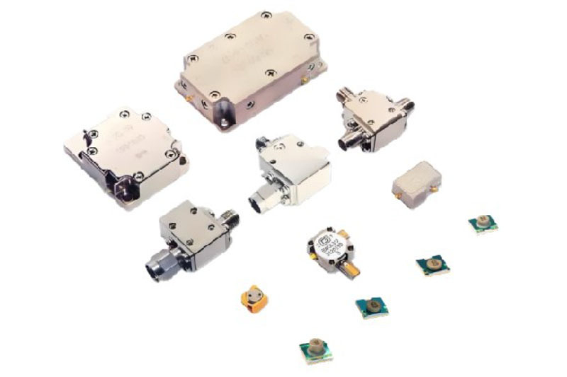
Features of MEMS Circulators
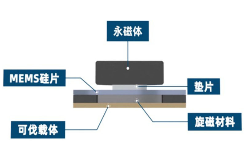
● Utilizing high-precision 3D MEMS fabrication technology to achieve silicon-based multilayer stacking and heterogeneous integration with magnetic materials, thereby enabling chip-level integration.
● Small size;
● Low loss;
● High power;
● Holds multiple invention patents.
● Typical value of insertion loss per section:
● 0.3 dB (X-band, Ku-band)
● 0.4 dB (Ka band)
● Typical power capacity:
● 100W (X-band, Ku-band)
● 30W (Ka-band)
Advantages of MEMS Circulators
● Unlike conventional microstrip circulators based on magnetic substrates, MEMS circulators employ a double-layer, low-loss, high-dielectric-constant single-crystal silicon material, integrated via MEMS technology with a heterostructure of ferrite magnetostrictive materials.
● Compared to conventional designs, MEMS circulators have a volume reduced by a factor of 10 and a weight reduced by a factor of 100. This leads to an overall system size reduction of up to 1,000 times—or even 10,000 times.
MEMS Circulator Applications

● Phased-array radar;
● Satellite communication;
● 5G/6G communication;
● Annual supply exceeds 1 million units.


Contact Phone
Contact Phone
Address
No.1, Meitai Road, Luquan District, Shijiazhuang City